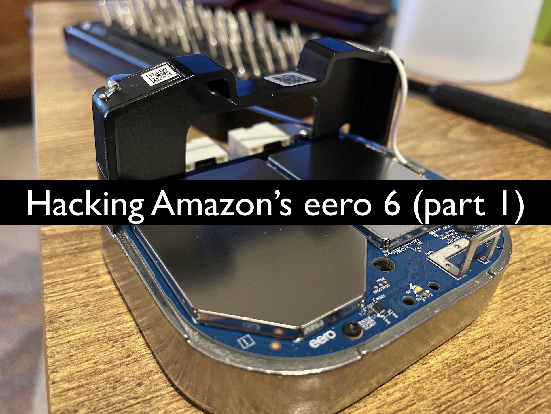
This is the first in the series of hacking Amazon’s eero 6 (3rd generation) Wi-Fi device. In this post I will be focusing on device disassembly, identifying pins, brute forcing JTAG, and reading serial output.
The second part of the blog can be found: https://markuta.com/eero-6-hacking-part-2/
About
Eero is a San Francisco-based wireless Internet company founded in 2015. It is known for making household consumer Wi-Fi products. The company was acquired by Amazon in 2019 for $97 million.
Device Specification
eero 6 (3rd gen 2020) device specification. The table below is based on data from evanmccann.net, which includes a nice table that compares other eero devices.
| Type | Value |
|---|---|
| CPU speed | 1.2GHz x 4 |
| CPU type | Cortex-A53 (Qualcomm IPQ6000) |
| RAM | 512MB |
| Storage | 4GB Flash (Kingston EMMC04G-M627) |
| Generation | Gen 3 |
| Release | 2020 |
| WiFi class | AX1800 (WiFi 6) |
| Type | Extender/Gateway |
| Radios | 2 (2.4GHz and 5GHz) |
| BlueTooth | 5.0 |
| ZigBee | Yes |
| Power | 15W (via USB type-C) |
FCC documents
Before purchasing a device on eBay, I first did a bit of research to find out whether there were any internal device photos available. I was mainly interested in anything resembling debug interfaces and chip part numbers. As it turns out, the Federal Communications Commission (FCC) published several documents of different eero products. These products were typically engineering samples but proved to be extremely useful.
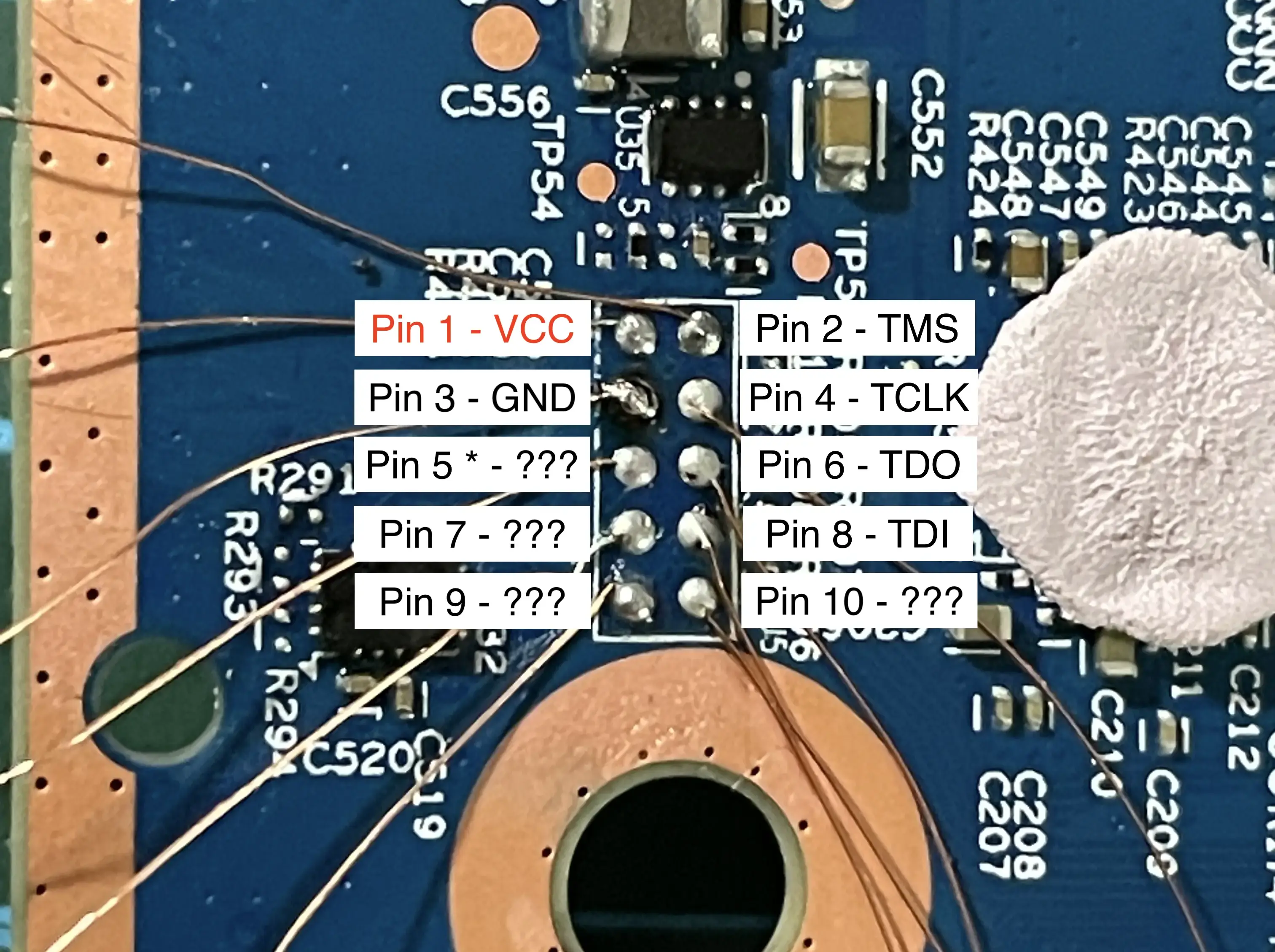
The documents (mirror available here) don’t have high resolution photos, which makes reading most chip markings difficult, but they did have a few photos of interesting pins. Here’s a photo that immediately peaked my interest.
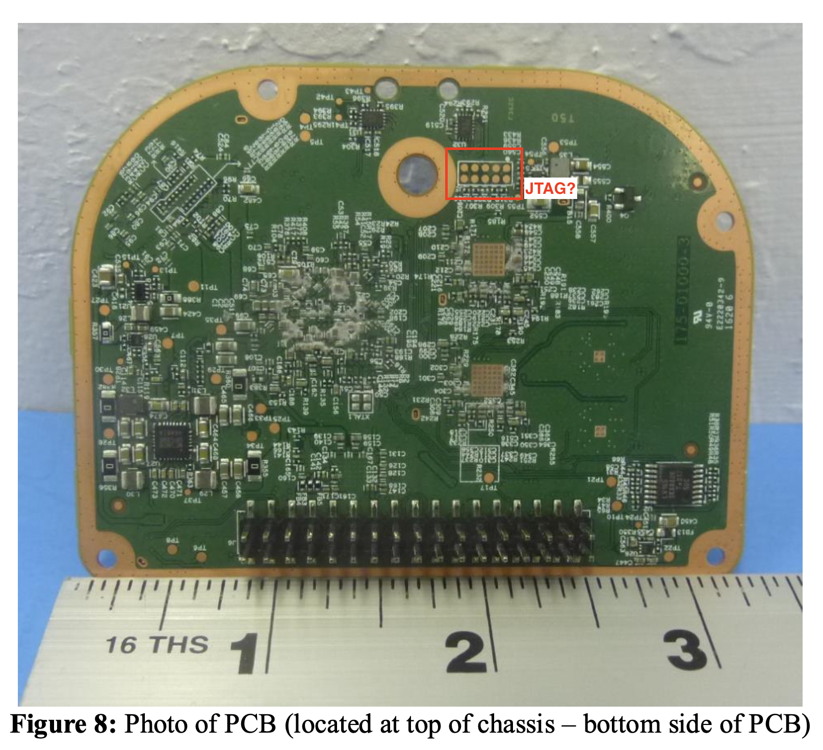 The 5 by 2 pins look a lot like a 10-pin ARM JTAG interface.
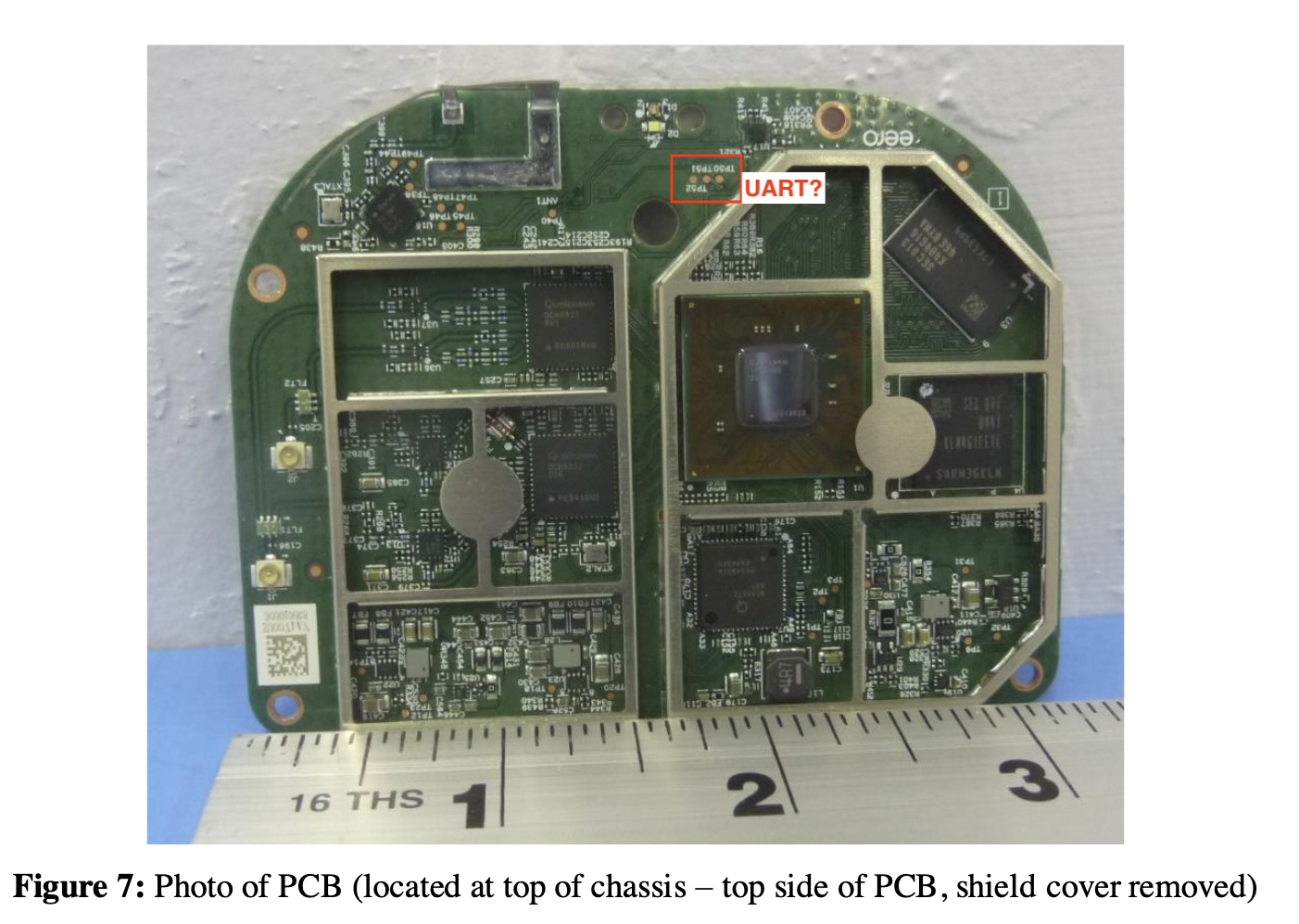
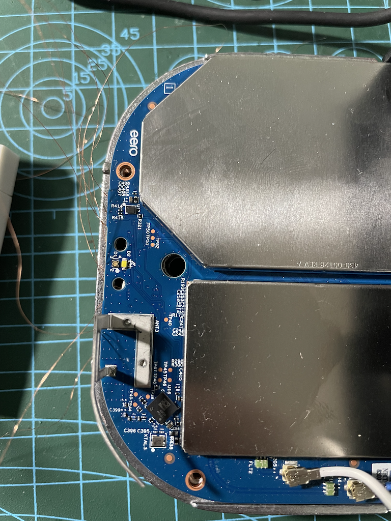
I also noticed 3 pins on the top side of the PCB, which looked like a serial interface.
Disassembly
The device itself was surprisingly easy to disassemble. To start off with you need to remove the manufacturer sticker located on the bottom of the device. This reveals a single T4? screw as shown in the photo below.
You then need to pry open the two plastic pieces, I used a thin piece of plastic (expired gift card) as to not damage internal components or the case itself. You will then see three T4 screws attached to the thick aluminum base.
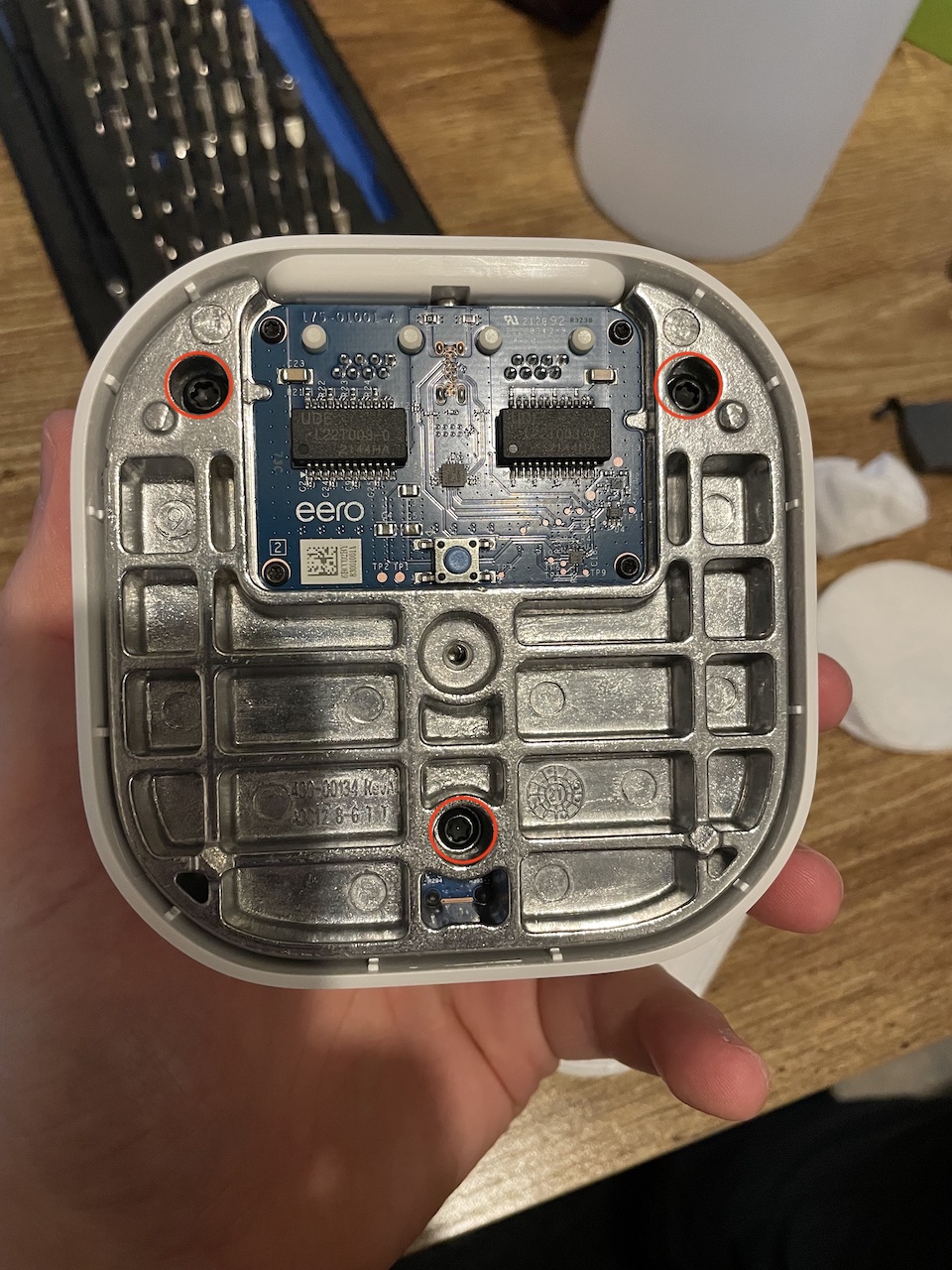
Flip the device over and remove four more screws.
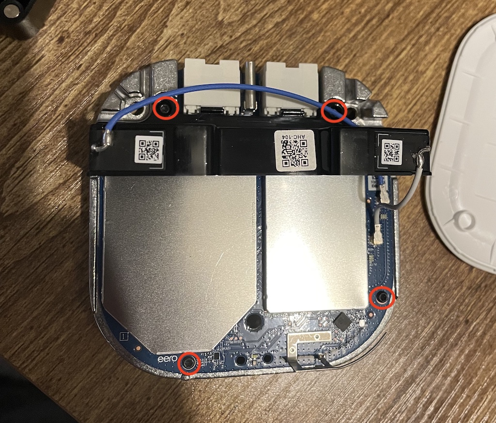
You will notice there are two main boards which are connected by a 34-pin GPIO interface. A board with two ethernet ports for networking and a single USB type-C port for power (15W). And the other board with the SoC, NAND, and other RF components.
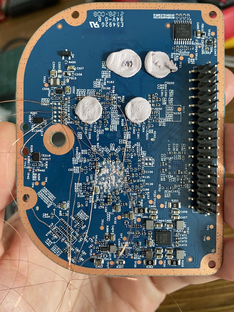
The following shows the underneath side of the board (one with the RF components).
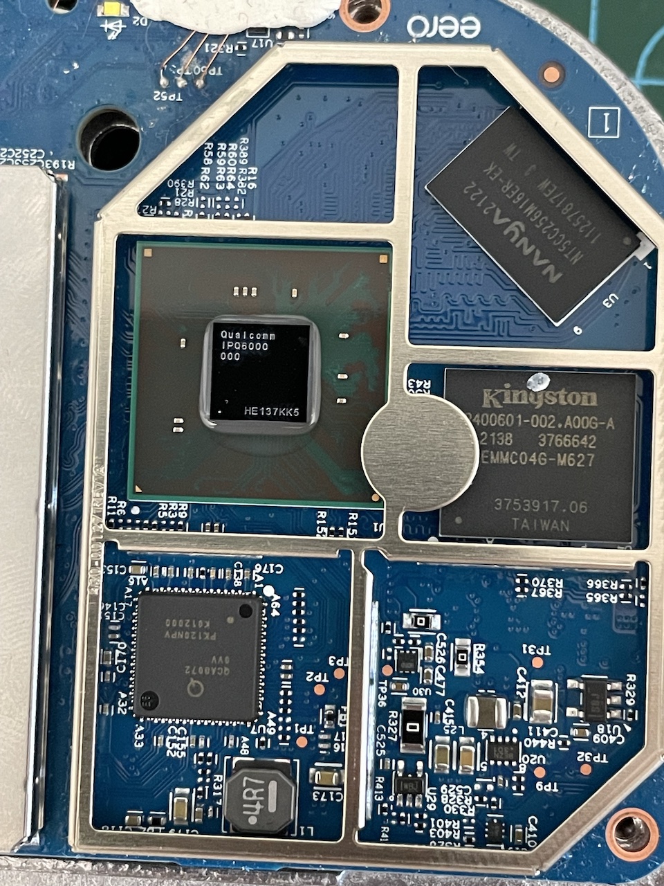
And here’s a view from the top with one of the RF shields removed, revealing the CPU, RAM and NAND chips:
Identifying pins
I quickly checked whether the same pins from the FCC photos were also present on my device, which they were. The only difference (it would seem) was that my PCB was blue, while the other one was green. It’s likely the FCC device was an engineering version.
Soldering wires
I soldered each pin onto a mini solder-able breadboard using a 0.2mm copper wire that had a thin layer of enamel. This made it much easier to work with as I could then attach it to a full size breadboard and then use standard jumper wires.
Before doing this I quickly checked for ground pins by putting my multimeter in continuity mode. I set my black probe on something I knew was ground like an RF shield, and the red probe on each pin.
A loud beep confirmed pin 3 was ground.
Here’s a photo of all the wires soldered onto a mini breadboard attached to my standard breadboard:
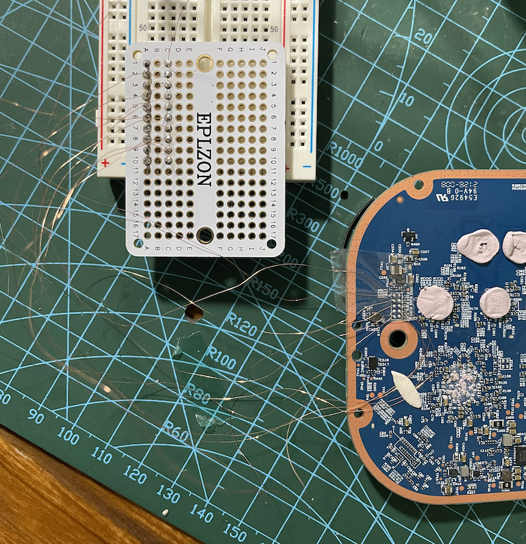
And here’s what it looked like with the two PCBs connected together, and wires protruding from underneath. I would later solder those 3 pins on the top (not seen in this photo):
Pin voltage
After soldering the wires to the breadboard I turned the device on and let to run for a few seconds. Here was the voltage I recorded for each pin:
Pin  Volts
1  - 1.8v
2  - 1.8v
3  - G
4  - 1.8v
5  - 0.5v
6  - 0.7v
7  - 0.4
8  - 1.8v
9  - 1.8v
10 - 1.8v
Setting up
Wiring
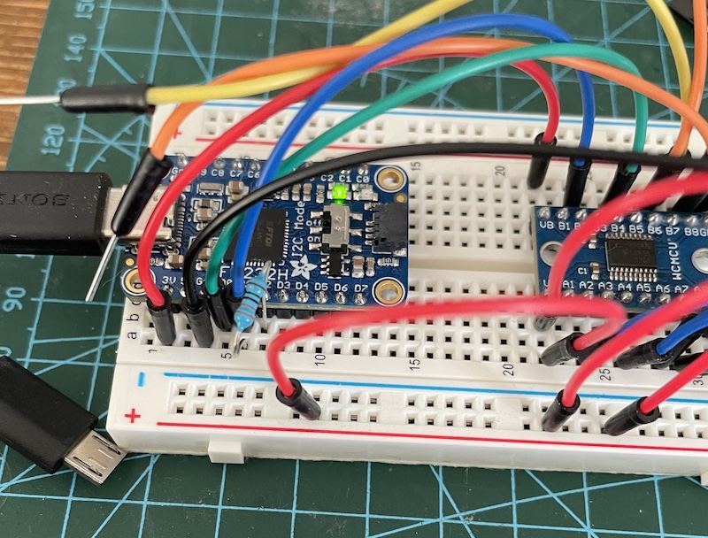
The wiring and pin numbers may get confusing, especially with multiple coloured pins, devices, and different orientations. I found it very useful to map out each pin in a small table and use it as a reference.
device | level shifter | Arduino  | program
-------+---------------+----------+--------
1 -----|    VA = VB    |---- 3.3v |
2 -----|    A1 = B1    |---- D2   | 1
3 ---- G               |          |
4 -----|    A2 = B2    |---- D3   | 2
5 -----|    A3 = B3    |---- D4   | 3
6 -----|    A4 = B4    |---- D5   | 4
7 -----|    A5 = B5    |---- D6   | 5
8 -----|    A6 = B6    |---- D7   | 6
9 -----|    A7 = B7    |---- D8   | 7
10 ----|    A8 = B8    |---- D9   | 8
Taking photos of the all the wires connected wasn’t very helpful, so I decided to create this diagram on how all of the components were connected:

Note: Also notice a little dot on the left side of pin 1 (1.8v line) on the eero device which indicates the first pin.
Logic level shifter
These 10-pins on the eero device operate under 1.8v, whereas the Arduino operates under 3.3v or 5v. I therefore needed to use a logic level shifter. A logic level shifter is a circuit board thats lets two devices that operate on a different voltage communicate with each other. A short video explanation here. I used an 8-channel shifter called TXS0108E.
Ardunio Nano
I also used a cheap little Arduino Nano RP2040 to act as my JTAG and SWD brute force tool. It was reprogrammed with two different platformio projects created by szymonh, one for JTAG called JTAGscan and the other for SWD called SWDscan.
Alternatively, you could use go-jtagenum, which works on Raspberry Pi models.
Brute force
The JTAGscan tool supports three different attack types (BYPASS, IDCODE, and BYPASS with just TDI). I made sure pins 2-8 were selected using the mask argument m with the value 0x1fc or 508 in decimal. Not seen in the output below, but I used the e enumerate option, and a to run all checks.
JTAG requires at least four (TCLK, TMS, TDI, and TDO) pins to operate, and for SWD it’s just two (SWCLK and SWDIO).
Note: The pin numbers in this section may be different from the previous sections.
> m
Enter pin mask 0x1fc
Pin mask set to 111111100

...
+-------------------------------+
|   4 |   2 |   6 |   8 |    32 |
+----------- SUCCESS -----------+
| TCK | TMS | TDO | TDI | Width |
+------ BYPASS complete --------+

...
+-------------------------------+
|   4 |   2 |   6 |    dba00477 |
+----------- SUCCESS -----------+
| TCK | TMS | TDO |      IDCODE |
+------ IDCODE complete --------+
    TCK, TMS, and TDO found.

...
+-- BYPASS searching, just TDI -+
| TCK | TMS | TDO | TDI | Width |
+-------------------------------+
|   4 |   2 |   6 |   8 |    32 |
+----------- SUCCESS -----------+
JTAG pins found! and the chip IDCODE of dba00477.
TCKis pin 4TMSis pin 2TDOis pin 6TDIis pin 8
SWDscan
Although not required, since we’ve already identified the JTAG interface which can be translated to TCLK = SWCLK and TMS = SWDIO. We can do it for the sake of completion.
Similar to the previous tool, here is the output:
> m
Enter pin mask 0x1fc
Pin mask set to 111111100
> e
+-------------------------------------------+
| CLK PIN | IO PIN | ACK | PART NO | MAN ID |
+-------------------------------------------+
|    2    |    3   |  7  |   ffff  |   7ff  |
|    2    |    4   |  7  |   ffff  |   7ff  |
|    2    |    5   |  7  |   ffff  |   7ff  |
|    2    |    6   |  7  |   ffff  |   7ff  |
|    2    |    7   |  7  |   ffff  |   7ff  |
|    2    |    8   |  7  |   ffff  |   7ff  |
|    3    |    2   |  7  |   ffff  |   7ff  |
|    3    |    4   |  7  |   ffff  |   7ff  |
|    3    |    5   |  7  |   ffff  |   7ff  |
|    3    |    6   |  7  |   ffff  |   7ff  |
|    3    |    7   |  7  |   ffff  |   7ff  |
|    3    |    8   |  7  |   ffff  |   7ff  |
|    4    |    2   |  1  |   ba02  |   23b  |
+----------------- SUCCESS -----------------+
Notice the manufacturer ID changes.
SWCLKis pin 4SWDIOis pin 2
Discoverd JTAG/SWD pinout
Debug interface
Now that we know the pins for both JTAG and SWD we need to use a debug adapter such as a Adafruit FT232H adapter (supports l2c, SPI, JTAG, UART etc.) to communicate with the eero device. The device is based on the widely supported FTDI chip, and works well under Linux tools.
OpenOCD
To communicate with discovered JTAG interface, I used the open-source utility OpenOCD. OpenOCD provides on-chip debugging, in-system programming, memory flashing, and boundary-scan testing. It supports a broad range of debugger adapters and it’s free, the catch is sometimes it can be a pain to configure, especially when the chip your trying to debug is unknown.
I used the latest version from and built from source.
My debugger.cfg adapter config for Adafruit FT232H (USB type-c) device:
# FT232H based USB-serial adaptor
#
# TCK:  D0
# TDI:  D1
# TDO:  D2
# TMS:  D3
# TRST: D4
# SRST: D5
# RTCK: D7

# speed
adapter speed 1000

# Setup driver type
adapter driver ftdi

# Common PID for FT232H
ftdi vid_pid 0x0403 0x6014
ftdi layout_init 0x0078 0x017b

# Set sampling to allow higher clock speed
ftdi tdo_sample_edge falling

# Reset pins
#ftdi layout_signal nTRST -ndata 0x0010 -noe 0x0040
#ftdi layout_signal nSRST -ndata 0x0020 -noe 0x0040

# debug mode either jtag or swd
transport select jtag
#transport select swd

#reset_config trst_only
I used a simple “probe” config for JTAG probe_jtag.cfg to identify chip IDs:
# JTAG adapter settings
script debugger.cfg

#scan_chain
init
dap info
shutdow
JTAG
naz@rasp4:~ $ sudo openocd -f debugger.cfg -f probe_jtag.cfg
Open On-Chip Debugger 0.12.0+dev-01082-gfc30feb51 (2023-03-12-23:07)
Licensed under GNU GPL v2
For bug reports, read
        http://openocd.org/doc/doxygen/bugs.html
trst_only separate trst_push_pull
Info : clock speed 1000 kHz
Warn : There are no enabled taps.  AUTO PROBING MIGHT NOT WORK!!
Info : JTAG tap: auto0.tap tap/device found: 0x5ba00477 (mfg: 0x23b (ARM Ltd), part: 0xba00, ver: 0x5)
Info : JTAG tap: auto1.tap tap/device found: 0x001390e1 (mfg: 0x070 (Qualcomm), part: 0x0139, ver: 0x0)
Warn : AUTO auto0.tap - use "jtag newtap auto0 tap -irlen 4 -expected-id 0x5ba00477"
Warn : AUTO auto1.tap - use "jtag newtap auto1 tap -irlen 11 -expected-id 0x001390e1"
Warn : gdb services need one or more targets defined
shutdown command invoked
OpenOCD found two TAP devices with the chip IDs 0x5ba00477 and 0x001390e1. I then used these values to attempted to create a new config file which tried to invoke these TAP interface.
Here’s my fourth attempt after reading wrongbaud’s post several times:
# Name of the SoC
if { [info exists CHIPNAME] } {
  set _CHIPNAME $CHIPNAME
} else {
  set _CHIPNAME qualcomm
}

# This is the TAP ID that we discovered in the previous step
if { [info exists CPUTAPID] } {
  set _CPUTAPID $CPUTAPID
} else {
  set _CPUTAPID 0x5ba00477
}

# Unknown at this point
#reset_config trst_only
#reset_config srst_only

# Here we create the JTAG TAP/DAP, defining the location and characteristics of our DAP
# add -ignore-syspwrupack

jtag newtap $_CHIPNAME cpu -irlen 4 -ircapture 0x1 -irmask 0xf -expected-id $_CPUTAPID
dap create $_CHIPNAME.dap -chain-position $_CHIPNAME.cpu -ignore-syspwrupack -adiv6

jtag newtap auto0 tap -irlen 11 -ircapture 0x1 -expected-id 0x001390e1
dap create auto0.dap -chain-position $_CHIPNAME.cpu -ignore-syspwrupack -adiv6

#set _TARGETNAME $_CHIPNAME.cpu
#set _TARGETNAME $_CHIPNAME.cpu.0

# Sort of working
target create $_CHIPNAME.dap.0 cortex_a -dap auto0.dap
target create lol cortex_a -dap $_CHIPNAME.dap

# Semi-working - testing
#target create lol cortex_m -dap $_CHIPNAME.dap -coreid 0
#target create lol2 cortex_m -dap auto0.dap

init
In another terminal window, I connected to the debug interface and issued a few DAP commands:
naz@rasp4:~ $ nc localhost 4444
Open On-Chip Debugger
> dap info 0
dap info 0
AP # 0x0
                AP ID register 0x14770004
                Type is MEM-AP AXI3 or AXI4
        MEM-AP BASE 0x00000002
                No ROM table present
> dap info 1
dap info 1
JTAG-DP STICKY ERROR
AP # 0x1
                AP ID register 0x44770002
                Type is MEM-AP APB2 or APB3
        MEM-AP BASE 0x80000000
                ROM table in legacy format
                Component base address 0x80000000
                Can't read component, the corresponding core might be turned off
> dap info 2
dap info 2
AP # 0x2
                AP ID register 0x24760010
                Type is JTAG-AP
> dap info 3
dap info 3
JTAG-DP STICKY ERROR
AP # 0x3
                AP ID register 0x24770011
                Type is MEM-AP AHB3
        MEM-AP BASE 0xe00ff003
                Valid ROM table present
                Component base address 0xe00ff000
                Can't read component, the corresponding core might be turned off
> dap info 4
AP # 0x4
                AP ID register 0x24770011
                Type is MEM-AP AHB3
        MEM-AP BASE 0xe00ff003
                Valid ROM table present
                Component base address 0xe00ff000
                Peripheral ID 0x04000bb4c3
                Designer is 0x23b, ARM Ltd
                Part is 0x4c3, Cortex-M3 ROM (ROM Table)
                Component class is 0x1, ROM table
                MEMTYPE system memory present on bus
        ROMTABLE[0x0] = 0xfff0f003
                Component base address 0xe000e000
                Peripheral ID 0x04000bb000
                Designer is 0x23b, ARM Ltd
                Part is 0x000, Cortex-M3 SCS (System Control Space)
                Component class is 0xe, Generic IP component
        ROMTABLE[0x4] = 0xfff02003
                Component base address 0xe0001000
                Invalid CID 0x00000000
        ROMTABLE[0x8] = 0xfff03003
                Component base address 0xe0002000
                Peripheral ID 0x04002bb003
                Designer is 0x23b, ARM Ltd
                Part is 0x003, Cortex-M3 FPB (Flash Patch and Breakpoint)
                Component class is 0xe, Generic IP component
        ROMTABLE[0xc] = 0xfff01003
                Component base address 0xe0000000
                Invalid CID 0xb1b1b1b1
        ROMTABLE[0x10] = 0xfff41002
                Component not present
        ROMTABLE[0x14] = 0xfff42003
                Component base address 0xe0041000
                Peripheral ID 0x04003bb924
                Designer is 0x23b, ARM Ltd
                Part is 0x924, Cortex-M3 ETM (Embedded Trace)
                Component class is 0x9, CoreSight component
                Type is 0x13, Trace Source, Processor
        ROMTABLE[0x18] = 0xfff45003
                Component base address 0xe0044000
                Peripheral ID 0x04004bb906
                Designer is 0x23b, ARM Ltd
                Part is 0x906, CoreSight CTI (Cross Trigger)
                Component class is 0x9, CoreSight component
                Type is 0x14, Debug Control, Trigger Matrix
                Dev Arch is 0x8ef00a14, DSL Memory "unknown" rev.0
        ROMTABLE[0x1c] = 0x00000000
                End of ROM table
Sadly, it looks like we don’t have access to all cores or that they have been disabled based on the JTAG-DP STICKY ERROR error. I was able to get a ram dump of some other component but it wasn’t the NAND flash where the device firmware is stored (disappointing).
SWD
To make SWD interface work properly with Adafruit FTDI 232H, I had to short pins D1 and D2 using a 330 Ohm resistor. Here’s what the wiring looked like:
- Pin
4was connected toD0 - Pin
2was connected toD1
And here’s the output produced by openocd:
naz@rasp4:~ $ sudo openocd -f probe_swd.cfg
Open On-Chip Debugger 0.12.0+dev-01082-gfc30feb51 (2023-03-12-23:07)
Licensed under GNU GPL v2
For bug reports, read
        http://openocd.org/doc/doxygen/bugs.html
Info : FTDI SWD mode enabled
Info : Listening on port 6666 for tcl connections
Info : Listening on port 4444 for telnet connections
Info : clock speed 200 kHz
Info : SWD DPIDR 0x5ba02477
Warn : gdb services need one or more targets defined
Strangely, the ID 0x5ba02477 was not the same as the one I saw earlier while trying to brute force.
Bonus (using J-link EDU)
I got annoyed at openocd - probably because I don’t know how to use it properly. So I decided to try a different one. I bought the industry standard JTAG debugger, the Segger J-Link debug adapter. I found a EDU mini on sale for around £60 on mouser.co.uk.
But I was still unsuccessful at getting the CPU to halt execution. Here’s the output:
SEGGER J-Link Commander V7.88c (Compiled May 16 2023 15:45:34)
DLL version V7.88c, compiled May 16 2023 15:43:58

Connecting to J-Link via USB...O.K.
Firmware: J-Link EDU Mini V1 compiled May 16 2023 10:45:21
Hardware version: V1.00
J-Link uptime (since boot): 0d 00h 14m 51s
S/N: 801044989
License(s): FlashBP, GDB
USB speed mode: Full speed (12 MBit/s)
VTref=3.266V


Type "connect" to establish a target connection, '?' for help
J-Link>connect
Please specify device / core. <Default>: ARM7
Type '?' for selection dialog
Device>?
Please specify target interface:
  J) JTAG (Default)
  S) SWD
  T) cJTAG
TIF>j
Device position in JTAG chain (IRPre,DRPre) <Default>: -1,-1 => Auto-detect
JTAGConf>
Specify target interface speed [kHz]. <Default>: 4000 kHz
Speed>200
Device "CORTEX-M3" selected.


Connecting to target via JTAG
TotalIRLen = 15, IRPrint = 0x0011
JTAG chain detection found 2 devices:
 #0 Id: 0x5BA00477, IRLen: 04, CoreSight JTAG-DP
 #1 Id: 0x001390E1, IRLen: 11, Unknown device
DAP: Could not power-up system power domain.
DPv0 detected
Scanning AP map to find all available APs
AP[5]: Stopped AP scan as end of AP map has been reached
AP[0]: AXI-AP (IDR: 0x14770004)
AP[1]: APB-AP (IDR: 0x44770002)
AP[2]: JTAG-AP (IDR: 0x24760010)
AP[3]: AHB-AP (IDR: 0x24770011)
AP[4]: AHB-AP (IDR: 0x24770011)
Iterating through AP map to find AHB-AP to use
AP[0]: Skipped. Not an AHB-AP
AP[1]: Skipped. Not an AHB-AP
AP[2]: Skipped. Not an AHB-AP
AP[3]: Skipped. Invalid implementer code read from CPUIDVal[31:24] = 0x00
AP[4]: Core found
AP[4]: AHB-AP ROM base: 0xE00FF000
CPUID register: 0x412FC231. Implementer code: 0x41 (ARM)
Found Cortex-M3 r2p1, Little endian.
FPUnit: 6 code (BP) slots and 2 literal slots
CoreSight components:
ROMTbl[0] @ E00FF000
[0][0]: E000E000 CID B105E00D PID 000BB000 SCS
[0][1]: E0001000 CID B105E00D PID 003BB002 DWT
[0][2]: E0002000 CID B105E00D PID 002BB003 FPB
[0][3]: E0000000 CID B105E00D PID 003BB001 ITM
[0][5]: E0041000 CID B105900D PID 003BB924 ETM-M3
[0][6]: E0044000 CID B105900D PID 004BB906 CTI
Memory zones:
  Zone: "Default" Description: Default access mode
Cortex-M3 identified.
J-Link>

J-Link>JTAGId
JTAG Id: 0x5BA00477  Version: 0x5 Part no: 0xba00 Man. Id: 023B
J-Link>reset
Reset delay: 0 ms
Reset type NORMAL: Resets core & peripherals via SYSRESETREQ & VECTRESET bit.
Reset: Halt core after reset via DEMCR.VC_CORERESET.
Reset: Reset device via AIRCR.SYSRESETREQ.
Reset: CPU may have not been reset (DHCSR.S_RESET_ST never gets set).
Reset: Using fallback: Reset pin.
Reset: Halt core after reset via DEMCR.VC_CORERESET.
Reset: Reset device via reset pin
Reset: VC_CORERESET did not halt CPU. (Debug logic also reset by reset pin?).
Reset: Reconnecting and manually halting CPU.
DAP: Could not power-up system power domain.
DPv0 detected
AP map detection skipped. Manually configured AP map found.
AP[0]: MEM-AP (IDR: Not set)
AP[1]: MEM-AP (IDR: Not set)
AP[2]: MEM-AP (IDR: Not set)
AP[3]: MEM-AP (IDR: Not set)
AP[4]: AHB-AP (IDR: Not set)
AP[4]: Core found
AP[4]: AHB-AP ROM base: 0xE00FF000
CPUID register: 0x412FC231. Implementer code: 0x41 (ARM)
Found Cortex-M3 r2p1, Little endian.
CPU could not be halted
Reset: Core did not halt after reset, trying to disable WDT.
Reset: Halt core after reset via DEMCR.VC_CORERESET.
Reset: Reset device via reset pin
Reset: VC_CORERESET did not halt CPU. (Debug logic also reset by reset pin?).
Reset: Reconnecting and manually halting CPU.
DAP: Could not power-up system power domain.
DPv0 detected
AP map detection skipped. Manually configured AP map found.
AP[0]: MEM-AP (IDR: Not set)
AP[1]: MEM-AP (IDR: Not set)
AP[2]: MEM-AP (IDR: Not set)
AP[3]: MEM-AP (IDR: Not set)
AP[4]: AHB-AP (IDR: Not set)
AP[4]: Core found
AP[4]: AHB-AP ROM base: 0xE00FF000
CPUID register: 0x412FC231. Implementer code: 0x41 (ARM)
Found Cortex-M3 r2p1, Little endian.
CPU could not be halted
CPU could not be halted

****** Error: Failed to halt CPU.
J-Link>
At this point I figured it’s time to move on, as I wasn’t getting anywhere. It’s very possible that an additional pin must be pulled up or down that activates the JTAG interface, but who knows… probably the manfacturers do.
Serial
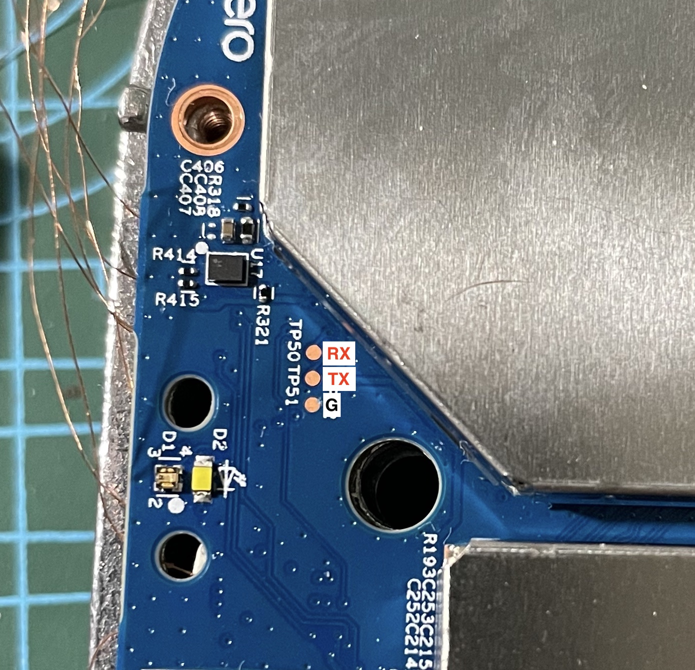 Those three pins on the top of the device were indeed a serial or UART interface, and after setting the correct baudrate
 115200 and TX & RX pins I was presented with the following output during bootup:
Format: Log Type - Time(microsec) - Message - Optional Info
Log Type: B - Since Boot(Power On Reset),  D - Delta,  S - Statistic
S - QC_IMAGE_VERSION_STRING=BOOT.XF.0.3-00089-IPQ60xxLZB-2
S - IMAGE_VARIANT_STRING=IPQ6018LA
S - OEM_IMAGE_VERSION_STRING=crm-ubuntu20
S - Boot Interface: eMMC
S - Secure Boot: On
S - Boot Config @ 0x000a602c = 0x000002e3
S - JTAG ID @ 0x000a607c = 0x001390e1
S - OEM ID @ 0x000a6080 = 0x007ab15b
S - Serial Number @ 0x000a4128 = 0x808edc43
S - Feature Config Row 0 @ 0x000a4130 = 0x0000800018200021
S - Feature Config Row 1 @ 0x000a4138 = 0x02c3e83783000009
S - PBL Patch Ver: 1
S - I-cache: On
S - D-cache: On
B -      3413 - PBL, Start
B -       592 - bootable_media_detect_entry, Start
B -      4339 - bootable_media_detect_success, Start
B -     52365 - elf_loader_entry, Start
B -     52535 - auth_hash_seg_entry, Start
B -     53716 - auth_hash_seg_exit, Start
B -     63087 - elf_segs_hash_verify_entry, Start
B -     89985 - elf_segs_hash_verify_exit, Start
B -     94168 - auth_xbl_sec_hash_seg_entry, Start
B -     94313 - auth_xbl_sec_hash_seg_exit, Start
B -    100648 - xbl_sec_segs_hash_verify_entry, Start
B -    100649 - xbl_sec_segs_hash_verify_exit, Start
B -    101578 - PBL, End
B -     86528 - SBL1, Start
B -    219935 - GCC [RstStat:0x0, RstDbg:0x600000] WDog Stat : 0x4
B -    222375 - clock_init, Start
D -      2806 - clock_init, Delta
B -    230915 - boot_flash_init, Start
D -     32116 - boot_flash_init, Delta
B -    266417 - sbl1_ddr_set_default_params, Start
D -       335 - sbl1_ddr_set_default_params, Delta
B -    272822 - boot_config_data_table_init, Start
D -      2287 - boot_config_data_table_init, Delta - (575 Bytes)
B -    281942 - CDT Version:2,Platform ID:8,Major ID:3,Minor ID:2,Subtype:144
B -    287523 - Image Load, Start
D -      6618 - OEM_MISC Image Loaded, Delta - (0 Bytes)
B -    297009 - Image Load, Start
D -      5063 - PMIC Image Loaded, Delta - (0 Bytes)
B -    304878 - sbl1_ddr_set_params, Start
B -    309941 - CPR configuration: 0x366
B -    313052 - Pre_DDR_clock_init, Start
D -       183 - Pre_DDR_clock_init, Delta
D -         0 - sbl1_ddr_set_params, Delta
B -    348005 - Image Load, Start
D -       427 - APDP Image Loaded, Delta - (0 Bytes)
B -    366122 - Image Load, Start
D -       427 - QTI_MISC Image Loaded, Delta - (0 Bytes)
B -    368714 - Image Load, Start
D -      7778 - Auth Metadata
D -       610 - Segments hash check
D -     19886 - QSEE Dev Config Image Loaded, Delta - (36498 Bytes)
B -    390705 - Image Load, Start
D -     13176 - Auth Metadata
D -     10279 - Segments hash check
D -    101626 - QSEE Image Loaded, Delta - (1435236 Bytes)
B -    492758 - Image Load, Start
D -      7625 - Auth Metadata
D -      1006 - Segments hash check
D -     22295 - RPM Image Loaded, Delta - (102676 Bytes)
B -    516395 - Image Load, Start
D -      7564 - Auth Metadata
D -      3233 - Segments hash check
D -     37058 - APPSBL Image Loaded, Delta - (576208 Bytes)
B -    581940 - SBL1, End
D -    495717 - SBL1, Delta
S - Flash Throughput, 39000 KB/s  (2151865 Bytes,  54250 us)
S - Core 0 Frequency, 800 MHz
S - DDR Frequency, 466 MHz


eero u-boot 1.2.7-0d393c56b2-l (Dec 11 2021 - 04:44:51 +0000)

DRAM:  smem ram ptable found: ver: 2 len: 4
512 MiB
NAND:  Could not find nand-flash in device tree
SF: Unsupported flash IDs: manuf 00, jedec 0000, ext_jedec 0000
ipq_spi: SPI Flash not found (bus/cs/speed/mode) = (0/0/48000000/0)
0 MiB
MMC:   <NULL>: 0 (eMMC)
PCI0 is not defined in the device tree
In:    serial@78B1000
Out:   serial@78B1000
Err:   serial@78B1000
model: [andytown-g]
machid: 8030290
eth0 MAC Address from ART is not valid
eth1 MAC Address from ART is not valid
eth2 MAC Address from ART is not valid
eth3 MAC Address from ART is not valid
eth4 MAC Address from ART is not valid
eth5 MAC Address from ART is not valid
board_register_value should be: 05
Net:   MAC0 addr:0:3:7f:ba:db:ad
PHY ID1: 0x4d
PHY ID2: 0xd0b2
EDMA ver 1 hw init
Num rings - TxDesc:1 (0-0) TxCmpl:1 (0-0)
RxDesc:1 (15-15) RxFill:1 (7-7)
ipq6018_edma_alloc_rings: successfull
ipq6018_edma_setup_ring_resources: successfull
ipq6018_edma_configure_rings: successfull
ipq6018_edma_hw_init: successfull
eth0
Warning: eth0 MAC addresses don't match:
Address in SROM is         00:03:7f:ba:db:ad
Address in environment is  c0:36:53:c5:1b:80

eero_boot:bootdelay enforced [0]
Hit any key to stop autoboot:  0
USB0:   Register 2000140 NbrPorts 2
Starting the controller
USB XHCI 1.10
scanning bus 0 for devices... 1 USB Device(s) found
USB1:   Register 1000140 NbrPorts 1
Starting the controller
USB XHCI 1.10
scanning bus 1 for devices... 1 USB Device(s) found
eero_boot:network boot disabled
eero_boot:booting usb
eero_boot:booting mmc
eero_boot:loading [eero_kernel.mbn] from partition [0:10]
sha1+ ## Loading kernel from FIT Image at 44000000 ...
   Using '[email protected]' configuration
   Trying 'kernel-1' kernel subimage
     Description:  Linux kernel
     Type:         Kernel Image
     Compression:  gzip compressed
     Data Start:   0x44000104
     Data Size:    14904410 Bytes = 14.2 MiB
     Architecture: ARM
     OS:           Linux
     Load Address: 0x41208000
     Entry Point:  0x41208000
     Hash algo:    sha1
     Hash value:   60081f4bab9232d1eb5347fe9274ccdda856984d
   Verifying Hash Integrity ... sha1+ OK
## Loading fdt from FIT Image at 44000000 ...
   Using '[email protected]' configuration
   Trying 'fdt-qcom-ipq6018-andytown-g.dtb' fdt subimage
     Description:  Flattened Device Tree blob
     Type:         Flat Device Tree
     Compression:  uncompressed
     Data Start:   0x44e36e6c
     Data Size:    70023 Bytes = 68.4 KiB
     Architecture: ARM
     Hash algo:    sha1
     Hash value:   0d37e519497e619feb18fb237b7041cf703daae0
   Verifying Hash Integrity ... sha1+ OK
   Booting using the fdt blob at 0x44e36e6c
   Uncompressing Kernel Image ... OK
   Loading Device Tree to 484eb000, end 484ff186 ... OK
Could not find PCI in device tree
Using machid 0x8030290 from environment

Starting kernel ...

[    0.000000] Booting Linux on physical CPU 0x0
[    0.000000] Initializing cgroup subsys cpuset
[    0.000000] Initializing cgroup subsys cpu
[    0.000000] Initializing cgroup subsys cpuacct
[    0.000000] Linux version 4.4.60-yocto-standard-eero (oe-user@oe-host) (gcc version 9.3.0 (GCC) ) #1 SMP PREEMPT Fri Feb 3 04:36:19 UTC 2023
[    0.000000] CPU: ARMv7 Processor [51af8014] revision 4 (ARMv7), cr=10c0383d
[    0.000000] CPU: PIPT / VIPT nonaliasing data cache, VIPT aliasing instruction cache
[    0.000000] Machine model: andytown-g
[    0.000000] Ignoring memory range 0x40000000 - 0x41000000
[    0.000000] cma: Reserved 28 MiB at 0x5e400000
[    0.000000] Memory policy: Data cache writealloc
[    0.000000] psci: probing for conduit method from DT.
[    0.000000] psci: PSCIv1.0 detected in firmware.
[    0.000000] psci: Using standard PSCI v0.2 function IDs
[    0.000000] psci: MIGRATE_INFO_TYPE not supported.
[    0.000000] PERCPU: Embedded 11 pages/cpu @9cf30000 s15436 r8192 d21428 u45056
[    0.000000] Built 1 zonelists in Zone order, mobility grouping on.  Total pages: 110244
[    0.000000] Kernel command line: ro systemd.verity_root_data=/dev/mmcblk0p18 systemd.verity_root_hash=/dev/loop10 roothash=d03330e57280e4481417b8146dc2be5af2559dfca299e67a4415fcb7e5305f7b fsck.repair=yes swiotlb=1 coherent_pool=2M
[    0.000000] PID hash table entries: 2048 (order: 1, 8192 bytes)
[    0.000000] Dentry cache hash table entries: 65536 (order: 6, 262144 bytes)
[    0.000000] Inode-cache hash table entries: 32768 (order: 5, 131072 bytes)
[    0.000000] Memory: 389508K/445440K available (6315K kernel code, 483K rwdata, 2056K rodata, 11264K init, 366K bss, 27260K reserved, 28672K cma-reserved, 0K highmem)
[    0.000000] Virtual kernel memory layout:
[    0.000000]     vector  : 0xffff0000 - 0xffff1000   (   4 kB)
[    0.000000]     fixmap  : 0xffc00000 - 0xfff00000   (3072 kB)
[    0.000000]     vmalloc : 0x9f800000 - 0xff800000   (1536 MB)
[    0.000000]     lowmem  : 0x80000000 - 0x9f000000   ( 496 MB)
[    0.000000]     pkmap   : 0x7fe00000 - 0x80000000   (   2 MB)
[    0.000000]     modules : 0x7f000000 - 0x7fe00000   (  14 MB)
[    0.000000]       .text : 0x80208000 - 0x80b2ce44   (9364 kB)
[    0.000000]       .init : 0x80c00000 - 0x81700000   (11264 kB)
[    0.000000]       .data : 0x81700000 - 0x81778d0c   ( 484 kB)
[    0.000000]        .bss : 0x8177b000 - 0x817d6858   ( 367 kB)
[    0.000000] SLUB: HWalign=64, Order=0-3, MinObjects=0, CPUs=4, Nodes=1
[    0.000000] Preemptible hierarchical RCU implementation.
[    0.000000] 	Build-time adjustment of leaf fanout to 32.
[    0.000000] NR_IRQS:16 nr_irqs:16 16
[    0.000000] Architected cp15 timer(s) running at 24.00MHz (virt).
[    0.000000] clocksource: arch_sys_counter: mask: 0xffffffffffffff max_cycles: 0x588fe9dc0, max_idle_ns: 440795202592 ns
[    0.000005] sched_clock: 56 bits at 24MHz, resolution 41ns, wraps every 4398046511097ns
[    0.000016] Switching to timer-based delay loop, resolution 41ns
[    0.000672] Calibrating delay loop (skipped), value calculated using timer frequency.. 48.00 BogoMIPS (lpj=240000)
[    0.000684] pid_max: default: 32768 minimum: 301
[    0.000776] Mount-cache hash table entries: 1024 (order: 0, 4096 bytes)
[    0.000786] Mountpoint-cache hash table entries: 1024 (order: 0, 4096 bytes)
[    0.001305] Initializing cgroup subsys io
[    0.001322] Initializing cgroup subsys memory
[    0.001346] Initializing cgroup subsys devices
[    0.001361] Initializing cgroup subsys freezer
[    0.001371] Initializing cgroup subsys net_cls
[    0.001381] Initializing cgroup subsys pids
[    0.001403] CPU: Testing write buffer coherency: ok
[    0.001765] CPU0: thread -1, cpu 0, socket 0, mpidr 80000000
[    0.001815] Setting up static identity map for 0x41300000 - 0x41300058
[    0.054348] MSM Memory Dump base table set up
[    0.054373] MSM Memory Dump apps data table set up
[    0.090260] CPU1: thread -1, cpu 1, socket 0, mpidr 80000001
[    0.120242] CPU2: thread -1, cpu 2, socket 0, mpidr 80000002
[    0.150274] CPU3: thread -1, cpu 3, socket 0, mpidr 80000003
[    0.150328] Brought up 4 CPUs
[    0.150349] SMP: Total of 4 processors activated (192.00 BogoMIPS).
[    0.150355] CPU: All CPU(s) started in SVC mode.
[    0.150739] devtmpfs: initialized
[    0.168648] VFP support v0.3: implementor 51 architecture 3 part 40 variant 3 rev 4
[    0.168950] clocksource: jiffies: mask: 0xffffffff max_cycles: 0xffffffff, max_idle_ns: 19112604462750000 ns
[    0.168976] futex hash table entries: 1024 (order: 4, 65536 bytes)
[    0.170182] pinctrl core: initialized pinctrl subsystem
[    0.171312] NET: Registered protocol family 16
[    0.173008] DMA: preallocated 2048 KiB pool for atomic coherent allocations
[    0.200103] cpuidle: using governor ladder
[    0.230121] cpuidle: using governor menu
[    0.230307] NET: Registered protocol family 42
[    0.245022] irq: no irq domain found for /soc/smp2p-wcss/slave-kernel !
[    0.248057] irq: no irq domain found for /soc/smp2p-wcss/slave-kernel !
[    0.257030] hw-breakpoint: found 5 (+1 reserved) breakpoint and 4 watchpoint registers.
[    0.257039] hw-breakpoint: maximum watchpoint size is 8 bytes.
[    0.258847] CPU: IPQ6000, SoC Version: 1.0
[    0.259603] qcom,cpr4-apss-regulator b018000.cpr4-ctrl: CPR valid fuse count: 4
[    0.260563] IPC logging disabled
[    0.260569] IPC logging disabled
[    0.260574] IPC logging disabled
[    0.260579] IPC logging disabled
[    0.260583] IPC logging disabled
[    0.260852] sps:sps is ready.
[    0.261582] console [pstore0] enabled
[    0.261590] pstore: Registered ramoops as persistent store backend
[    0.261599] ramoops: attached 0x100000@0x50100000, ecc: 0/0

----[CUT]----
You can find the full serial log at eero-6-serial-output.txt
From the serial output, we know that:
- Uses U-Boot version
1.2.7-0d393c56b2-l - Secure boot enabled
- Can’t interrupt boot sequence :(
- SoC is a Qualcomm IPQ6000 datasheet - requires virtual points :(
Summary
This was an on and off project, that lasted a few months, where I would find time after my day job. I’ve learned a lot but there’s still more to learn. This project definately sparked my curiosity into hardware hacking again. But I can’t say I wasn’t a bit disappointed at not being to extract the flash firmware or getting a shell. Maybe in part 2 ;)
I hope somebody finds this post useful and that they can continue research.
Next steps
Try bypass the U-BOOT secure boot protection, to at least get a shell through interrupting the boot process or dump the firmware image. Figure out the right sequence for configuring the JTAG interface and halt the main CPU. Test out fault injection attacks. De-solider the Kingston (EMMC04G-M627) NAND chip to extract the firmware.